This last week I put a lot of effort into finalizing the schematics and ensuring that the board will work the way that we want them to perform. Here's a couple of photos of the full schematics.
 |
| Master schematic, which shows connections between the chipKIT and all of the layers. |
 |
| Full layer schematic. |
|
|
|
|
|
|
|
|
|
|
|
|
|
|
More details on each of the schematics will follow after the break.
First off, let's look at the Master schematic. The master schematic features 3 distinct sections: the chipKIT, the line drivers, and all of the layers.
It was decided that each layer would require 2 serial lines for a 45% increase in speed. Other than the separate serial lines, every layer shares the same data lines. The naming conventions for each serial line follow this pattern: Panel(P)#_Serial Line(S)#. So, the first Serial In line for panel 7 would appear as P7_S1.

Also included are the other 10 signal lines in common with every layer. These lines are located on PORTE. These signals, go to line drivers. We were worried about fanout, so we put each one of these common lines to a line driver. The line drivers chosen were 74LS241. The circuit diagram is shown to the right. Each chipKIT pin drives 2 input lines on the 241's. This in turn drives 2 output pins on the line driver, which controls 12 panels of LEDs and chips.
A small example of the panels appears like the image suggests on the left. This shows the inner 2 rows of panels and the connections it makes with the above 2 images.
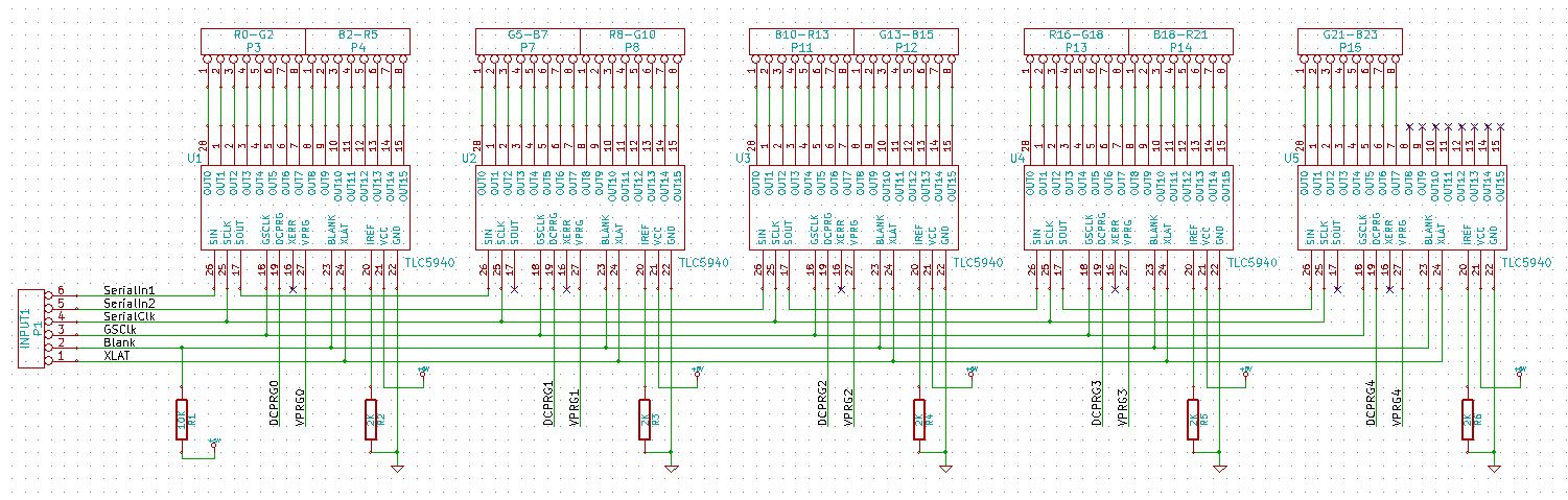
Finally, one also must understand the layer schematics. The following 4 photos show how this works.
This schematic reveals how power filtering for each layer will take place. Each layer has a Schottky diode. It also has filtering for high and low frequency noise.
It was decided to still have the functionality of being able to program the dot correction and other features in EEPROM while not taking up pins on the chipKIT. Therefore, jumpers are provided on each layer. This allows someone to manipulate the jumpers, write the data out to EEPROM, and then shift the jumpers back to lock it into PWM mode for normal operation.
This photo shows the ground side including the PWM chips. The only change between an early photo of the schematics and this one is the pull-up resistor on the BLANK line. This forces the PWM chips to be blanked during the 3 seconds that the bootloader takes to start up on the chipKIT.
Nothing so far has been done to the Power side of this schematic. I have this presently built on the breadboard, but have not yet gotten the chance to sit down and work on it because other commitments have gotten in the way. That is my next task in the software design is to get the demuxes working. Once I have that, I will rework the software to be the fast version, using the direct port writing as opposed to digital writes (which are extremely slow in the Arduino environment).


 Also included are the other 10 signal lines in common with every layer. These lines are located on PORTE. These signals, go to line drivers. We were worried about fanout, so we put each one of these common lines to a line driver. The line drivers chosen were 74LS241. The circuit diagram is shown to the right. Each chipKIT pin drives 2 input lines on the 241's. This in turn drives 2 output pins on the line driver, which controls 12 panels of LEDs and chips.


No comments:
Post a Comment